


Here is a comprehensive overview of the project, structured into a formal call/program announcement for prospective participants.
---
# Project Overview: Atomic-Level Engineering of Ultra-Thin Ferroelectric Hafnium Oxide ($HfO_2$) for 3D Storage-Class Memory
## 🔬 Project Focus & Context
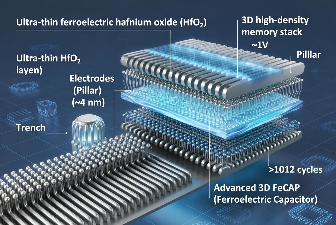
This cutting-edge research initiative centers on the **atomic-level engineering of ultra-thin ferroelectric hafnium oxide ($HfO_2$)**, aiming for its seamless integration into high-density 3D storage-class memory.
As next-generation data-centric applications—such as Artificial Intelligence (AI) and edge computing—demand ever-higher performance, $HfO_2$-based ferroelectrics present a game-changing opportunity due to their low-power consumption, high density, and excellent scalability. To unlock this potential, this project actively addresses critical industry bottlenecks, including high write voltages, physical scaling limitations, and endurance constraints.
### Key Objectives & Innovations
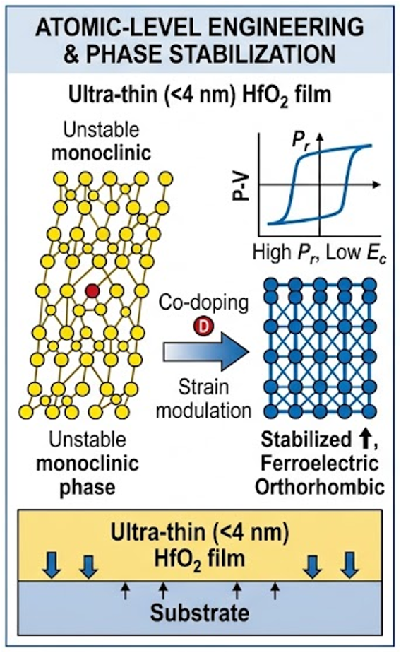
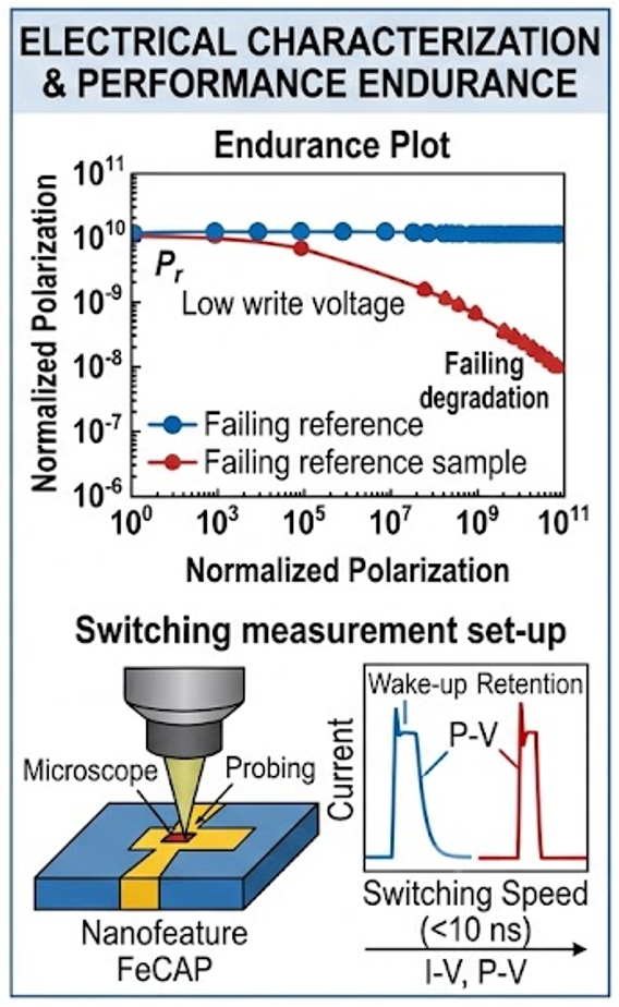
* **Target:** Develop ultra-thin ($<4 ext{ nm}$) $HfO_2$-based ferroelectric capacitors (FeCAPs).
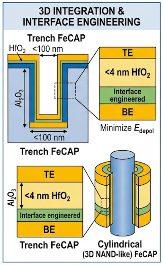
* **Architectures:** Integration into advanced 3D designs, specifically trench, pillar, and cylindrical structures.
* **Core Strategies:** Employ advanced co-doping strategies to stabilize the ferroelectric orthorhombic phase, utilize interface engineering to minimize unwanted depolarization fields, and implement precise strain modulation to maximize overall device performance.
---
## 📋 Program Details & Participant Provisions
### ⏱️ Schedule & Duration
* **Duration:** A fixed commitment of **5 to 6 months** is required.
* This timeline ensures participants can see a core R&D cycle through, from initial atomic-level synthesis/simulation to device characterization.
### 💰 Scholarships & Financial Support
* **Monthly Stipend:** Participants will receive a scholarship/stipend of **NTD 12,000 to NTD 15,000 per month**.
* This financial aid is intended to offset living costs and local expenses during the research stay.
### 🏠 Accommodation Arrangements
* **Housing:** Assistance with housing arrangements will be provided. Depending on campus/facility availability, participants will be given access to university dormitories or guided placement in verified off-campus student housing. *(Note: Exact sub-rates or utility fees are typically subsidized or covered out of the monthly stipend).*
---
## 🎓 Participation Requirements
### 1. Educational Background & Majors
* **Target Audience:** Open to advanced undergraduate (Senior), Master’s, or Ph.D. level students.
* **Relevant Fields:** A strong academic background in **Electrical Engineering, Materials Science and Engineering, Solid-State Physics, Nanotechnology**, or closely related microelectronics disciplines.
### 2. Core Technical Competencies
Prospective candidates should ideally possess familiarity or an interest in expanding their skills in:
* Thin-film deposition techniques (such as Atomic Layer Deposition / ALD).
* Semiconductor device characterization (e.g., electrical testing, polarization-voltage looping, or C-V measurements).
* Fundamental understanding of crystallography, phase transitions (specifically the orthorhombic phase), and semiconductor physics.
### 3. Language Proficiency
* **Requirement:** Professional working proficiency in **English** is mandatory.
* Because this is an internationalized, high-level R&D environment, the capability to review scientific literature, present data, and collaborate on technical documentation in English is crucial.
---
## ⚠️ Important Considerations for Participants
* **Intellectual Property & Confidentiality:** Given the highly competitive nature of next-generation 3D memory technologies (AI/Edge hardware), participants will be required to adhere to standard lab confidentiality agreements regarding proprietary co-doping and interface engineering data.
* **Hands-on Lab Safety:** Working with nanoscale fabrication and thin-film equipment requires strict adherence to cleanroom and chemical safety protocols. Training will be provided upon arrival.
* **Visa Timeline:** Because the duration is 5–6 months, international researchers must coordinate their visa application early to ensure a valid entry permit aligned with the project's start date.
![]()
- Field: Engineering
- School: National Tsing Hua University
- Organizer: College of Semiconductor Research
- Period of Apply: 2026/07/01-2026/12/31
- Term: 2026/07/01-2026/12/31

- Contact Person:Sourav De
- Email:sourav.de@mx.nthu.edu.tw