


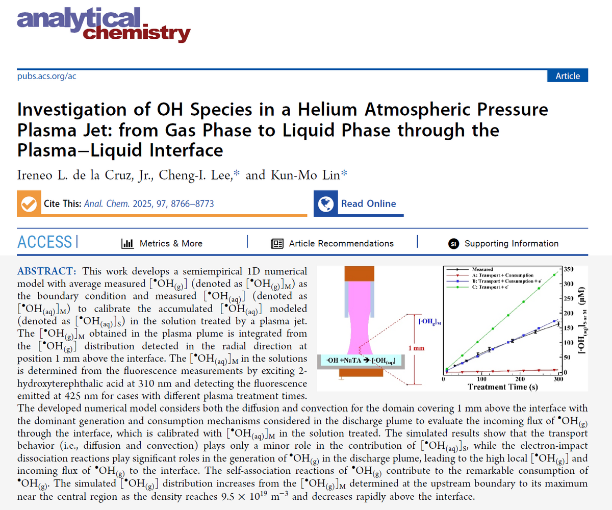
Project abstract:
Plasma technology plays a crucial role in modern semiconductor manufacturing, enabling precise, efficient, and scalable processes. In microelectronics fabrication, plasma is widely used for dry etching (PEALE), deposition (PECVD/PEALD), surface modification, and cleaning. Plasma etching is one of the most critical steps for defining nanoscale patterns on silicon wafers. By generating reactive species such as ions and radicals, plasma can selectively remove material with excellent anisotropy, allowing the creation of vertical sidewalls and high-aspect-ratio structures essential for advanced devices. Compared to wet chemical etching, plasma etching offers superior process control, uniformity, and compatibility with small feature sizes. In this project, participants are going to work with a low-pressure discharge system using instruments to measure discharge parameters and conduct theoretical analyses. Specific tasks will be assigned to resolve engineering issues and contribute to the ongoing project with domain knowledge learned in lecture courses.
Internship period: 2-3 months
Background: Department of Mechanical Engineering is preferred
![]()
- Field: Engineering
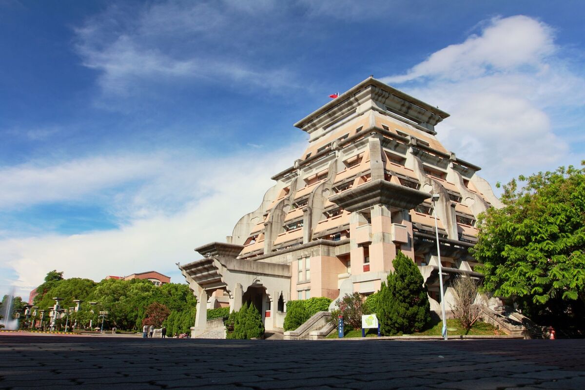
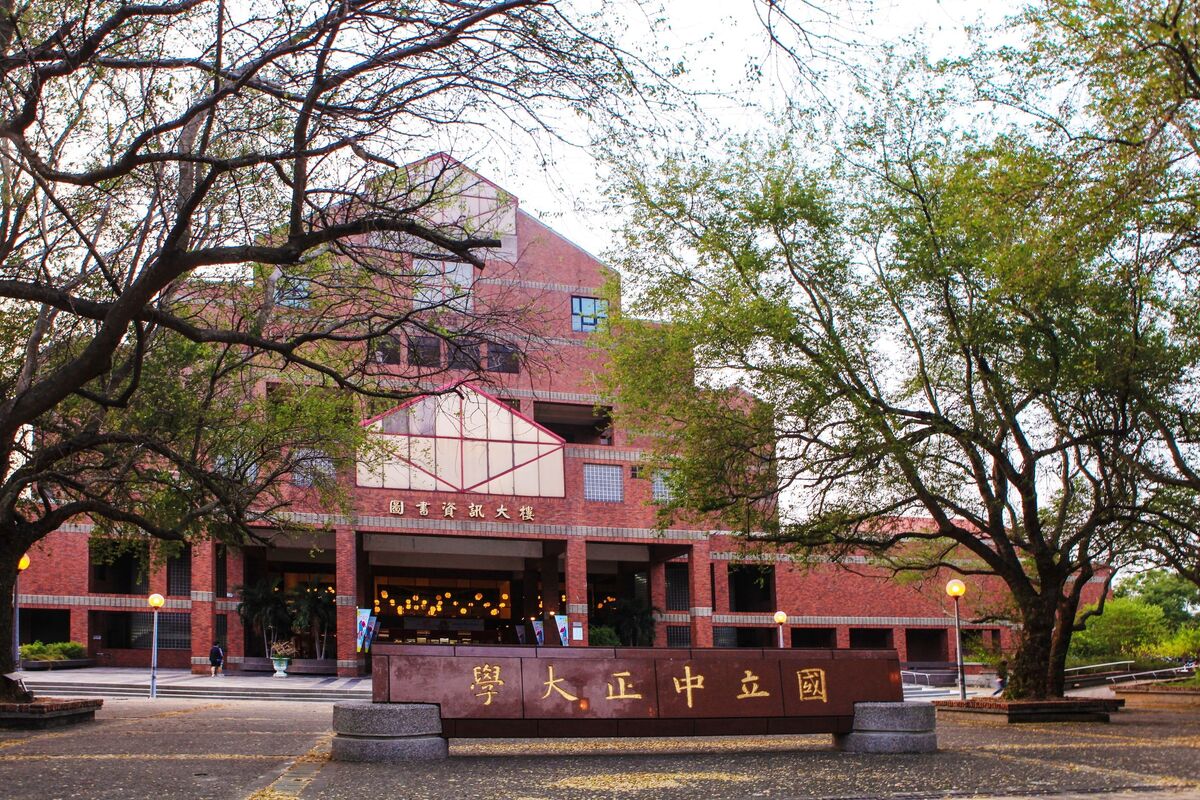
- School: National Chung Cheng University
- Organizer: Department of Mechanical Engineering
- Period of Apply: 2026/04/01-2026/12/15
- Term: 2-3 months
- Fee: Scholarship or Self-funded

- Contact Person:Kun-Mo Lin
- Email:kmlin.tw@gmail.com