


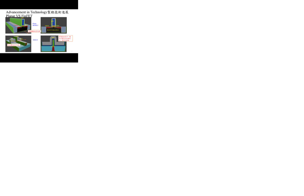
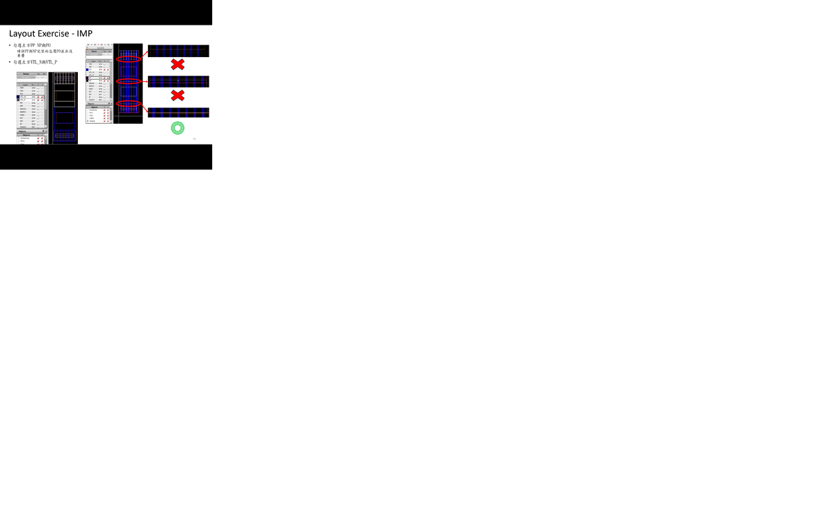
1. Integrating Machine Learning (ML) into CMOS Layout design is a high-impact research area often referred to as "Intelligent Physical Design." 2. In modern CMOS (especially FinFET), the "Layout-vs-Schematic" (LVS) and "Design Rule Check" (DRC) loops are incredibly slow. Designers often finish a layout only to find that parasitic resistance/capacitance has ruined the timing, or that they have hundreds of DRC violations. 3. This proposal aims to build a Predictive Surrogate Model that gives instant feedback during the drawing phase. 4. The following objectives outline a project focused on using ML to automate and optimize the most time-consuming parts of the CMOS layout flow. 5. Objectives (1) Predict Parasitics: Use Graph Neural Networks (GNN) to predict wire resistance and capacitance directly from a partial layout. (2) DRC Hotspot Detection: Use Computer Vision (CNN/U-Net) to identify areas likely to fail design rules before running heavy verification tools (like Calibre). (3) Active Learning: Implement a feedback loop where the model learns from every manual correction a designer makes. 6. Reference: (1) https://github.com/gdsfactory/gdsfactory 7. Example: (1) Phase 1: Dataset Generation Use GDSFactory to generate 1,000 variations of an Inverter or NAND gate layout with varying wire widths. (2) Phase 2: Training a DRC Predictor Convert GDSII files to PNG images (e.g. using gds2png scripts). (3) Label pixels that fail DRC (e.g., "Metal spacing too small"). (4) Train a simple U-Net in PyTorch. (5) Comparison
![]()
- Field: Engineering
- School: Feng Chia University
- Organizer: Depart. of Electronics
- Period of Apply: 2026/04/01-2026/09/01
- Term: 2026/07/01-
- Fee: 1. No Accommodation Provided
2. Rant fee: ~5000NT$/Month

- Contact Person:Ching-Hwa Cheng
- Email:chengch@fcu.edu.tw
- Phone:+886-4-24517250~4963