


With the development of Sub-6GHz, the scaling down of HEMT components to meet Sub-6GHz requirements has become a competitive technology among major manufacturers worldwide. However, this gate scaling process introduces a short-channel effect, impacting the high-frequency characteristics of nitride components. This project aims to utilise InAlN/GaN HEMTs from domestic semiconductor wafer foundries, where the indium content is 17%, almost perfectly matching the GaN lattice, making it a new option for next-generation nitride RF circuits. Using Keysight's ADS high-frequency circuit design software, a circuit design combining a T-gate HEMT with a transimpedance amplifier (TIA) and a multi-stage Class-F/E power amplifier (PA) is implemented. The TIA circuit utilises differential and symmetrical structures to eliminate diffusion current generated by the substrate, achieving low noise and overall bandwidth coverage across all 6G communication ranges.
![]()
- Field: Engineering
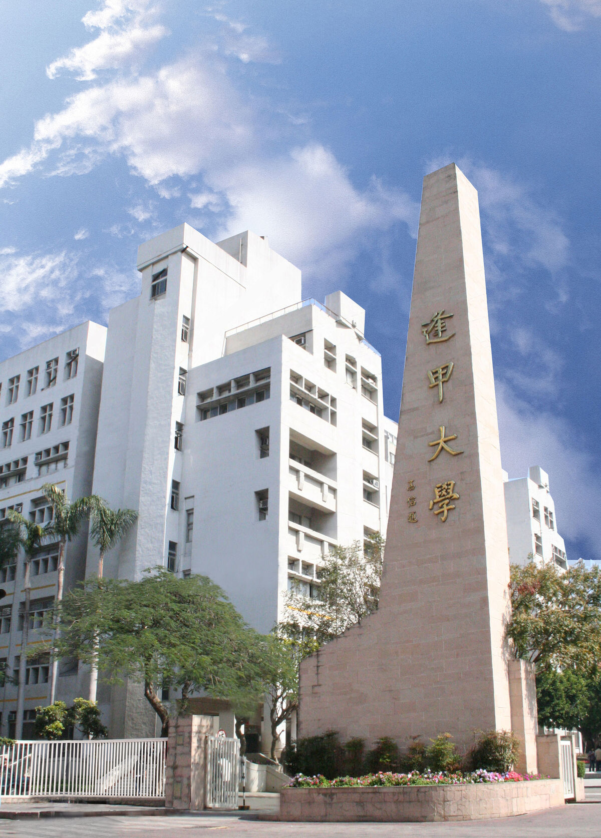
- School: Feng Chia University
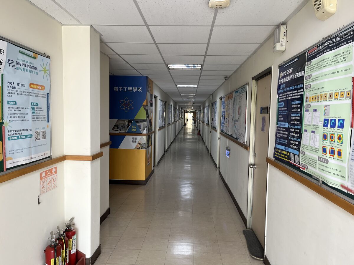
- Organizer: Department of Electronic Engineering
- Period of Apply: 2026/03/30-2026/12/31
- Term: 2026/03/30-2026/12/31
- Fee: The interns need to pay for their daily expenses by themselves, including meals, accommodation, and transportation.
- Website of Program: scholar.google.com/citations?hl=zh-TW&user=sx9ECC0AAAAJ

- Contact Person:Tong-Wen Wang
- Email:tongwwang@fcu.edu.tw
- Phone:+886-937-791265